KAWASAKI, Japan, Mar 27, 2026 - (JCN Newswire) - Fujitsu today announced the development of a world-leading, high-sensitivity and high-resolution infrared sensor to expand monitoring capabilities in the defense and disaster prevention fields. This sensor is a Type-II superlattice (T2SL) infrared sensor with over 1 million pixels, capable of detecting both mid-wavelength infrared (MWIR) and long-wavelength infrared (LWIR) light. Its high-sensitivity allows it to clearly capture minute thermal differences of 0.05°C or less, enabling high-precision monitoring day and night. This over 1-megapixel dual-band T2SL infrared sensor is the first of its kind in the world.
The newly developed technology boasts dramatically enhanced detection and identification performance, with applications spanning a wide range of fields. For example, when applied to optical sensor systems mounted on satellites or aircraft, it can contribute to the creation of new value across diverse areas, including early assessment of disaster situations and environmental monitoring.
Integrating this sensor into monitoring devices for defense and disaster prevention enables accurate detection of thermal changes, such as identifying precursors to human activity or object movement, locating people during disasters, detecting early forest fires, and monitoring tsunamis. This contributes to improving information gathering capabilities and strengthening defense and disaster prevention. Additionally, by visualizing thermal distribution and changes over time with exceptional precision, the sensor is anticipated to play a vital role in tackling societal issues like infrastructure inspection and problems with analytical equipment, while also driving progress in scientific research.
This technology was developed under contract as part of the "PROTOTYPE OF WIDE BAND AND HIGH RESPONSIVITY PHOTO-DETECTORS" from Acquisition Technology & Logistics Agency (ATLA), Japan Ministry of Defense, to which Fujitsu has completed delivery of the prototype sensor.
Starting in fiscal year 2026, Fujitsu plans to leverage the manufacturing technology of this sensor to develop new products and market them for use in monitoring cameras.
Background
In the security sector, which underpins a safe and secure society, there is a demand for advanced sensing technologies that can detect various threats early and accurately capture their precursors. However, with the diversification of monitoring scenarios and the increasing complexity of targets, there is a need for even higher resolution sensors and improved identification capabilities through simultaneous detection of multiple wavelengths. The ATLA initiated a research prototype project to establish technology that enables target detection and identification over longer distances and wider areas than existing systems. Fujitsu, which has developed and mass-produced high-sensitivity infrared sensors, was awarded this project and has now successfully completed its development.
Overview of the developed sensor
Infrared sensors capture infrared radiation spontaneously emitted by objects with heat, visualizing their surface temperature distribution. Fujitsu has leveraged the characteristics of T2SL, a compound semiconductor with a superlattice structure that allows for material property control, to develop a unique dual-band sensor. The superlattice structure, where different semiconductor materials are layered at the nanometer (one billionth of a meter) level, offers high sensitivity, as well as excellent control over detection wavelengths and manufacturability. By selecting a combination of semiconductor materials with a large energy offset in their band structure (i.e., Type-II Superlattice, T2SL), it is possible to detect infrared light, which has lower energy than visible light.
This sensor can detect MWIR and LWIR wavelength bands, with high-sensitivity capable of detecting temperature differences of 0.05°C or less. By simultaneously detecting two wavelengths with a single pixel, it can accurately detect and identify targets that would otherwise be obscured by background noise during detection with single-wavelength sensors. Furthermore, by advancing miniaturization of elements through the development of manufacturing processes and mounting technologies suitable for delicate T2SL materials, Fujitsu has achieved high-resolution with over 1 million pixels, enabling the capture of more distant targets.
This infrared sensor, simultaneously achieving high-sensitivity, high-resolution, and dual-band detection, is suitable for monitoring applications in defense, disaster prevention, and other fields requiring high discrimination performance.
Furthermore, this world-first technology from Fujitsu will drive further advancements in the sensitivity, multi-band and high-resolution capabilities of conventional infrared sensors, enabling a diverse range of product developments.
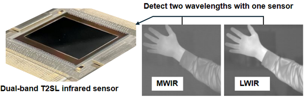
Figure: Dual-band T2SL infrared sensor and example images
About Fujitsu
Fujitsu’s purpose is to make the world more sustainable by building trust in society through innovation. As the digital transformation partner of choice for customers around the globe, our 113,000 employees work to resolve some of the greatest challenges facing humanity. Our range of services and solutions draw on five key technologies: AI, Computing, Networks, Data & Security, and Converging Technologies, which we bring together to deliver sustainability transformation. Fujitsu Limited (TSE:6702) reported consolidated revenues of 3.6 trillion yen (US$23 billion) for the fiscal year ended March 31, 2025 and remains the top digital services company in Japan by market share. Find out more: global.fujitsu
Press Contacts
Fujitsu Limited
Public and Investor Relations Division
Inquiries
Topic: Press release summary
Source: Fujitsu Ltd
Sectors: Electronics, Aerospace & Defence
http://www.acnnewswire.com
From the Asia Corporate News Network
Copyright © 2026 ACN Newswire. All rights reserved. A division of Asia Corporate News Network.
|