|
| Monday, 5 December 2016, 16:09 HKT/SGT | |
| |  | |
Source: Fujitsu Ltd | |
|
|
|
|
| Achieves up to a doubling of write speeds, improving the response speed of virtual desktops and speeding up database processing |
KAWASAKI, Japan, Dec 5, 2016 - (JCN Newswire) - Fujitsu Laboratories Ltd. today announced the development of a high-speed in-memory data deduplication technology for all-flash arrays, which are large-scale, high-speed storage systems and use multiple flash devices such as solid-state drives. This technology enables the production of storage systems with up to twice the response speed when writing data, compared to previous methods.
 | | Figure 1: All-Flash Array Storage System and Deduplication
|
 | | Figure 2: New In-Memory Deduplication Technology |
 | | Figure 3: Network load leading to drop in write response speed |
 | | Figure 4: Response performance improvement with the newly developed method.
|
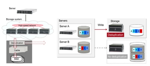
In recent years, all-flash arrays have incorporated deduplication technology that consolidates duplicate data into one to write to a flash device, in order to utilize the limited capacity of flash devices. However, as the system connects to multiple flash devices through a network in order to search for duplicate data each time it writes data, and storage devices grow in capacity and increase in speed, a problem of lowered response speed during write operations arises.
Now Fujitsu Laboratories has developed a new method that can accelerate response speeds by executing deduplication after writing data. In addition, as data may be written to memory twice in some cases when processing is continued with the new method, thereby increasing communications volume and lowering overall processing performance, Fujitsu Laboratories has developed technology to automatically switch between the new method and the previous method, as operational conditions require.
This means that response speeds can be increased by up to two times, improving the response of virtual desktop services and reducing database processing times.
Details of this technology were announced at the 28th Computer Systems Symposium (ComSys2016), held November 28 at Hosei University in Tokyo.
Development Background
In recent years, with the advance of virtualization and the use of big data in business, performance requirements for storage systems have been increasing. All-flash arrays, which can increase performance by using high-speed flash devices and connecting multiple devices with a high-speed network, have therefore become widely used.
Flash devices are more expensive than traditional hard drives, and can only be written to a limited number of times over their lifetime, so all-flash arrays incorporate deduplication functionality that consolidates data to write only once to the flash device, which can increase the actual volume and reduce the number of unnecessary write operations (Figure 1).
http://www.acnnewswire.com/topimg/Low_FujitsuStorage1251.jpg
Figure 1: All-Flash Array Storage System and Deduplication
Issues
In order to utilize expensive flash devices effectively, in-memory deduplication technology was developed for all-flash arrays featuring deduplication functionality. However, because previous technology would institute a process to search for duplicate data before writing through a network that connects multiple flash devices, with storage systems that grow in capacity and increase in speed it created issues with longer response times when writing data due to the overhead required for search processing.
About the Technology
Fujitsu Laboratories has developed a technology that can improve response speed for in-memory deduplication up to two times (Figure 2).
http://www.acnnewswire.com/topimg/Low_FujitsuStorage1252.jpg
Figure 2: New In-Memory Deduplication Technology
Details of the technology are as follows.
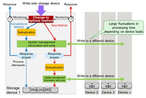
1. New deduplication technology that improves response speed under low load
With the newly developed deduplication technology, the storage devices that make up the all-flash array cooperate to complete a write operation by temporarily storing the write data in open memory (the cache), improving response times. Then, while the server is preparing for the next write operation depending on the response from the memory, the technology searches for duplicate data, communicating between the storage devices in parallel, and the data is finally written to the solid-state drive after duplicates are eliminated. With this technology, response times for write operations can improve by up to two times when the storage system's network load is low.
2. Response time optimization technology actively switches between two deduplication methods
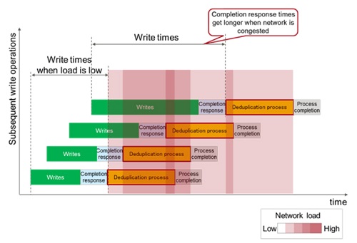
Deduplicating after responding improves response speed compared to previous methods when the storage system's network load is low, but when the load is high the network becomes congested. This reduces response times more than previous methods due to data writes across multiple devices taking longer (Figure 3).
With the newly developed response time optimization technology, of the two deduplication methods, the original method that writes after deduplication, for which the response time does not greatly vary, and the newly developed method, for which response times vary widely, the system automatically chooses the method with the shortest response time by calculating the expected value for the average response time, based on records measuring the actual response time.
http://www.acnnewswire.com/topimg/Low_FujitsuStorage1253.jpg
Figure 3: Network load leading to drop in write response speed
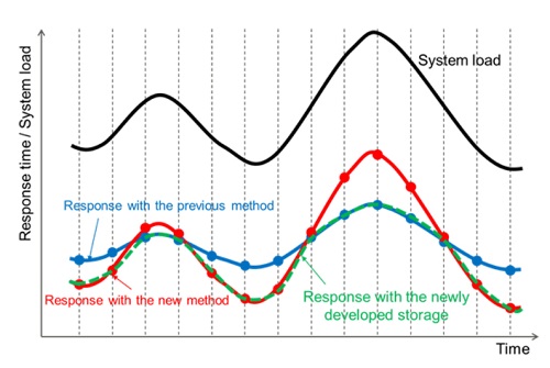
With this technology, by automatically choosing the optimal method in response to the continually changing status of the system, it is possible to reduce system response time as a whole (Figure 4).
http://www.acnnewswire.com/topimg/Low_FujitsuStorage1254.jpg
Figure 4: Response performance improvement with the newly developed method.
Effects
Using the newly developed technology, Fujitsu Laboratories was able to achieve a lowest latency of about half that of previous technology in fio(1) benchmarks. As a result, Fujitsu Laboratories was able to increase response speed when writing data to an all-flash array by up to two times For example, in applications such as virtual desktops and data base processing that require high write speeds, as accessing small files occurs in enormous volumes, there are many duplications. In such situations, user applications on the service could be sped up, improving the user experience. In addition, by applying this system to back-end storage for operations databases, operations systems could be sped up, enabling further consolidation of IT infrastructure.
Future Plans
Fujitsu Laboratories will continue development of technologies to further accelerate all-flash arrays going forward, aiming to incorporate them into Fujitsu Limited's storage products from fiscal 2017 or later.
(1) fio: flexible I/O tester
A benchmark tool used to measure storage performance. It generates read/write load based on designated settings, and produces detailed performance data output.
About Fujitsu Laboratories
Founded in 1968 as a wholly owned subsidiary of Fujitsu Limited, Fujitsu Laboratories Ltd. is one of the premier research centers in the world. With a global network of laboratories in Japan, China, the United States and Europe, the organization conducts a wide range of basic and applied research in the areas of Next-generation Services, Computer Servers, Networks, Electronic Devices and Advanced Materials. For more information, please see: http://www.fujitsu.com/jp/group/labs/en/.
Contact:
Fujitsu Laboratories Ltd.
Computer Systems Laboratory
E-mail: afa-pr-2016@ml.labs.fujitsu.com

Fujitsu Limited
Public and Investor Relations
Tel: +81-3-3215-5259
URL: www.fujitsu.com/global/news/contacts/
Topic: Press release summary
Source: Fujitsu Ltd
Sectors: Electronics
http://www.acnnewswire.com
From the Asia Corporate News Network
Copyright © 2026 ACN Newswire. All rights reserved. A division of Asia Corporate News Network.
|
|
|

|
|
|
|
| Fujitsu Ltd |
| Mar 25, 2026 09:58 HKT/SGT |
|
Fujitsu and The University of Osaka develop new technologies for chemical material energy calculations on early-FTQC quantum computers |
| Mar 24, 2026 13:01 HKT/SGT |
|
Fujitsu and Umios conduct joint pilot project for electronic traceability system to visualize seafood distribution |
| Mar 23, 2026 13:24 HKT/SGT |
|
Fujitsu-developed traffic simulation system utilized in Maebashi City's public transportation planning |
| Mar 16, 2026 11:55 HKT/SGT |
|
Fujitsu Japan and Teikyo University Hospital launch joint proof of concept to build mechanism for data analysis and referred-patient management |
| Mar 10, 2026 10:45 HKT/SGT |
|
Fujitsu launches Japan's first defense tech open innovation program |
| Mar 9, 2026 12:32 HKT/SGT |
|
Fujitsu and DT-Axis collaborate to advance digital health |
| Mar 3, 2026 20:00 HKT/SGT |
|
Fujitsu and BCN Port Innovation Foundation leverage ocean digital twin technology to drive the regeneration of the Port of Barcelona |
| Mar 2, 2026 10:55 HKT/SGT |
|
Fujitsu supports sustainable growth for retailers with data and AI through Uvance for Retail |
| Feb 27, 2026 11:03 HKT/SGT |
|
Fujitsu POS solution enhances customer experience at Hankyu Hanshin Department Stores |
| Feb 25, 2026 11:00 HKT/SGT |
|
Beisia Automates Supermarket Refrigerator Temperature Monitoring and Recording with Fujitsu's IoT Visualization Solution |
| More news >> |
 |
|
|
|