|
|
|
|
|
|
| Contributing to improved manufacturing productivity for semiconductor devices by optimizing processes and improving yields |
TOKYO, Dec 14, 2021 - (JCN Newswire) - Hitachi High-Tech Corporation today announced the Development of its Electron Beam Area Inspection System GS1000. This, newly developed tool, offers precise and fast e-beam inspection by using common platform, which is based on proven Hitachi High-Tech's high-speed inspection SEM's, Hitachi High-Tech's expertise in market leading CD-SEM(1) technology, and high-speed and massive measurements.
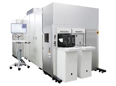 | | Electron Beam Area Inspection System GS1000 |
Demand for the cutting-edge semiconductor devices mass-production is being drastically increased, driving introduction of EUV Lithography to enable smaller semiconductor devices. Hitachi High-Tech is contributing to the increased productivity in modern semiconductor industry by providing fast e-beam GS1000 system to facilitate massive metrology over a wide inspection area.
Development Background:
Shrinking of semiconductor device nodes is continuing with cutting-edge device manufacturers introducing EUV(2) technology, which is capable of quick and extremely precise lithography. The device manufacturers are beginning to utilize this technology in the mass production of 5nm node devices and the development of 3nm node devices. As circuit pattern dimensions manufactured using EUV lithography are approximately half of the size of those produced by ArF(3) lithography, systems that can inspect and measure these smaller patterns reliably, accurately and in a repeatable manner have become essential to managing production lines and yields. Particularly, quality assurance of advanced EUV masks to reduce variations in circuit dimensions and randomly occurring microscopic stochastic*4 defects characteristic of EUV lithography becomes of an utmost importance. Consequently, the need for high-throughput, high-resolution inspection and measurements is increasing in line with the expansion of number of inspection targets.
Hitachi High-Tech is responding to this increased demand for high-speed, sensitive inspection and measurements over a wide area and is launching GS1000 system to fulfil the needs of semiconductor device mass-production market.
Key Features:
GS1000 is an advanced conventional Electron Beam Inspection (EBI(5)) system. It is a fusion of a high-performance electron optical system and a high-speed, large-capacity data processing system, which provides solutions to the challenges that arise when introducing EUV lithography to semiconductor device mass-production.
This system has the following key features:
1. New technology capable of a high-speed, wide-area e-beam inspection
By using optical aberration correctors developed through advanced electron optical system designs, wafers can be imaged by electron beam with no degradation of resolution within a wide area of the electron beam movement, enabling high-precision inspection and measurements over a wide area. This system uses a combination of a fast-changing field of view using beam shift and a sensitive inspection technology to enable high-precision, wide-area scans 100 times faster than conventional CD-SEM tools.
2. High-speed, large-capacity image processing system
Dedicated high-speed image processing system provides ultra-fast data transfer enabling high throughput, performing real-time D2DB measurements(6) through parallel processing using high-speed 4K imaging and image transfer servers. It also introduces D2AI algorithmic inspection(7), utilizing AI(8) technology to handle processing of the vast amounts of data created by the increasing number of points being inspected and measured to meet the needs of fast detection of process variation and microscopic defects.
Hitachi High-Tech is working to meet customers' needs in metrology and inspection for the R&D and mass production of semiconductor devices by supplying electron beam-based products such as traditional CD-SEM and wafer inspection systems based on optical technologies. Hitachi High-Tech will continue to provide innovative solutions for the upcoming technology challenges. Hitachi High-Tech will contribute to the development of cutting-edge technologies by creating new social and environmental value in collaboration with its customers.
(1) CD-SEM: Scanning Electron Microscope (SEM) for measuring the microscopic circuit patterns on semiconductor wafers. Used for inspections on semiconductor devices development and production lines, these systems are essential for yield management.
(2) EUV (Extreme Ultraviolet): An extreme ultraviolet light source with a wavelength of 13.5 nm.
(3) ArF: An ArF excimer laser (wavelength 193 nm) light source.
(4) Stochastic defects: Defects that occur randomly, which have been a particular problem in the development of EUV lithography technology.
(5) EBI: Electron Beam Inspection: Wafer inspection equipment that uses electron beams.
(6) D2DB Measurement: Die to Database Measurement: An algorithmic procedure that performs comparative inspections and measurements between areas printed of the wafer (the die) and the configured design data for the same area.
(7) D2AI Algorithmic Inspection: Die to AI Inspection: An algorithmic process for inspecting areas of the wafer (the die) using AI.
(8) AI: Artificial Intelligence. A field of computer science that artificially recreates assorted human perceptions and human intelligence using the concepts of calculation and computation.
About Hitachi High-Tech
Hitachi High-Tech, headquartered in Tokyo, Japan, is engaged in activities in a broad range of fields, including Analytical & Medical Solutions (manufacture and sales of clinical analyzers, biotechnology products, and analytical instruments), Nano-Technology Solutions (manufacture and sales of semiconductor manufacturing equipment and analysis equipment), and Industrial Solutions (providing high value-added solutions in fields of social & industrial infrastructures and mobility, etc.).
The company's consolidated revenues for FY 2020 were approx. JPY 606.3 billion [USD 5.7 billion]. For further information, visit http://www.hitachi-hightech.com/global/.
Topic: Press release summary
Source: Hitachi, Ltd.
Sectors: Electronics
http://www.acnnewswire.com
From the Asia Corporate News Network
Copyright © 2026 ACN Newswire. All rights reserved. A division of Asia Corporate News Network.
|
|
|

|
|
|
|
| Hitachi, Ltd. |
| Apr 21, 2026 18:21 HKT/SGT |
|
Hitachi to establish a new company with Nojima under a strategic partnership to accelerate growth of its home appliance business |
| Apr 15, 2026 17:17 HKT/SGT |
|
Hitachi Energy and Samsung C&T expand strategic collaboration to accelerate grid infrastructure and reinforce energy security |
| Apr 3, 2026 10:09 HKT/SGT |
|
Hitachi Rail announces agreement to acquire Clever Devices, marking its growth as a global digital mobility player |
| Mar 31, 2026 18:14 HKT/SGT |
|
Hitachi Digital Services Strengthens OT-IT Integration with Manufacturing Operations Management Platform |
| Mar 30, 2026 18:21 HKT/SGT |
|
MOL and Hitachi Launch Initiative to Convert Used Ships into Floating Data Centers |
| Mar 27, 2026 18:44 HKT/SGT |
|
Hitachi and MUFG Bank expand NextGen model to finance vehicles and charging infrastructure for decarbonized mobility |
| Mar 26, 2026 21:10 HKT/SGT |
|
OKI and Hitachi Agree to Integrate Businesses Related to Automated Teller Machines (ATMs) and Other Automated Equipment |
| Mar 26, 2026 14:13 HKT/SGT |
|
Hitachi Rail to manufacture rolling stock for Seibu Railway"s new Fine Dining Train |
| Mar 24, 2026 17:07 HKT/SGT |
|
HIES introduces plant-based lubricant that reduces air compressor lifecycle CO(2) emissions by 40% |
| Mar 23, 2026 10:49 HKT/SGT |
|
Hitachi Receives the 2026 Catalyst Award, a Global Recognition for Building an Inclusive Organization |
| More news >> |
 |
|
|
|