|
|
|
|
|
|
| In-Line Wafer Surface Inspection System to Improve Yield and Reduce Inspection Costs |
TOKYO, Dec 13, 2022 - (JCN Newswire) - Hitachi High-Tech Corporation announced today the launch of the LS9600, a new system for detecting particles and defects on non-patterned wafer surfaces. It features a new high-output, short-wavelength laser that improves throughput at the sensitivity levels required for the mass production of cutting-edge semiconductor devices by approx. 2.6 times compared to our previous generation systems. By introducing this product, Hitachi High-Tech will continue to help to improve yields and reduce inspection costs associated with customers' mass production of semiconductor devices.
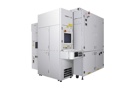 | | Wafer Surface Inspection System LS9600 |
Development Background
Non-patterned wafer inspection systems are used for applications such as controlling the condition (cleanliness) of non-patterned wafers to manage particles and defects in semiconductor device manufacturing equipment. Due to the shrinking of semiconductor devices, the defects of interest (DOIs), which impact yield during the manufacturing process, have also become smaller in size. As a result, there is a growing need for high-sensitivity inspection that can detect DOIs of 20 nm and smaller across the entire surface of non-patterned wafers. In addition to high-sensitivity inspection to improve yield, there is also a strong demand for high throughput, which leads to lower inspection costs.
Key New Technologies
This system achieves both high sensitivity and high throughput by implementing the following new technologies.
1. High-Output, Short-Wavelength Laser
The deep-ultraviolet laser has a higher output and shorter wavelength than legacy systems, which increases the amount of light scattered by microscopic defects, thereby achieving a higher degree of sensitivity.
2. New Optical Detection System
The new optical detection system features a larger surface area to capture light scattered by DOIs compared to the legacy systems. In addition, its newly developed high-sensitivity sensor has improved the detection rate of weak scattered light by around 20%.
3. New Data Processing System
Improved scattered light data-processing algorithms deliver higher sensitivity, together with higher throughput due to high-speed, real-time data processing.
By using this product, as well as our wafer optical inspection systems, and electron beam-based products such as a traditional CD-SEM(1) and DR-SEM(2), Hitachi High-Tech is working to meet customers' various needs in processing, measurement, and inspection throughout the semiconductor manufacturing process. We will continue to provide innovative and digitally enhanced solutions to our products for the upcoming technology challenges, and create new value together with our customers, as well as contributing to cutting-edge manufacturing.
(1) CD-SEM (Critical Dimension-Scanning Electron Microscope): An equipment for measuring the microscopic circuit patterns on semiconductor wafers. Used for inspections on semiconductor devices development and production lines, these systems are essential for yield management.
(2) DR-SEM (Defect Review-Scanning Electron Microscope): An equipment for reviewing the microscopic circuit patterns and defects on semiconductor wafers. Used for inspections on semiconductor devices development and production lines, these systems are essential for yield management.
About Hitachi High-Tech
Hitachi High-Tech, headquartered in Tokyo, Japan, is engaged in activities in a broad range of fields, including manufacture and sales of clinical analyzers, biotechnology products, and analytical instruments, semiconductor manufacturing equipment and analysis equipment. and providing high value-added solutions in fields of social & industrial infrastructures and mobility, etc. The company's consolidated revenues for FY 2021 were approx. JPY 576.8 billion [USD 5.1 billion]. For further information, visit www.hitachi-hightech.com/global/
Contact:
Yuuki Minatani
Business Planning Dept., Metrology Systems Div.,
Nano-Technology Solution Business Group, Hitachi High-Tech Corporation
E-mail: yuki.minatani.dc@hitachi-hightech.com
Topic: Press release summary
Source: Hitachi, Ltd.
Sectors: Electronics
http://www.acnnewswire.com
From the Asia Corporate News Network
Copyright © 2025 ACN Newswire. All rights reserved. A division of Asia Corporate News Network.
|
|
|

|
|
|
|
| Hitachi, Ltd. |
| Oct 1, 2025 19:37 HKT/SGT |
|
The Second Proton Therapy System Begins Treatment at University of Tsukuba Hospital |
| Oct 1, 2025 18:33 HKT/SGT |
|
Hitachi Energy invests an additional $270 million CAD ($195 million USD) to expand large power transformer manufacturing capacity in Varennes, Quebec |
| Sept 26, 2025 18:46 HKT/SGT |
|
Hitachi Announces NVIDIA AI Factory to Accelerate Physical AI Innovation |
| Sept 25, 2025 18:01 HKT/SGT |
|
Entered a partnership with ELITech in the Field of Molecular Testing for Infectious Disease |
| Sept 24, 2025 18:46 HKT/SGT |
|
Hitachi agrees to acquire German data and AI services firm synvert to accelerate Agentic AI and Physical AI development, driving global expansion of HMAX business |
| Sept 11, 2025 17:35 HKT/SGT |
Hitachi accelerates growth with major U.S. investments in advanced manufacturing, electrification and workforce development
|
| Sept 11, 2025 16:24 HKT/SGT |
|
GlobalLogic and Ericsson Deploy Private 5G Network at Hitachi Rail's State-of the-Art Digital Factory |
| Sept 11, 2025 15:46 HKT/SGT |
|
GlobalLogic and Flexware Innovation Announce Major Deployment of LIFT at Hitachi Rail's State-of-the-Art Train Manufacturing Facility |
| Sept 5, 2025 20:00 HKT/SGT |
|
Hitachi announces historic $1 billion USD manufacturing investment to power America's energy future through production of critical grid infrastructure |
| Sept 2, 2025 10:50 HKT/SGT |
|
Hitachi has been certified as a Gold Partner of Scaled Agile, Inc., the provider of the large-scale agile framework "SAFe(R)" |
| More news >> |
 |
|
|
|