|
|
|
|
|
|
| - High radiation tolerance and ultra-low power consumption - |
TOKYO, Mar 7, 2017 - (JCN Newswire) - NEC Corporation and the National Institute of Advanced Industrial Science and Technology (AIST) today announced the development of an NB-FPGA(1) that incorporates NanoBridge metal atom migration-type switch technology utilizing TIA(2), an open innovation hub operated by five institutes in Tsukuba and Tokyo. This original NEC product featuring high radiation tolerance is expected to contribute to the use of LSIs in space.
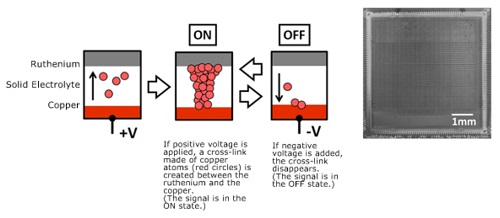
 | | Figure 1: Operation mechanism of NanoBridge (left), NB-FPGA chip (right) |
Current FPGAs (SRAM-type FPGAs)(3), when used in space, pose the problem of changes occurring to the information written in the SRAM and malfunctions being caused due to the effects of radiation. However, this NanoBridge technology enables a tenfold improvement over the power efficiency of conventional FPGAs as well as providing them with high radiation tolerance.
NEC has conducted an operation demonstration jointly with the Japan Aerospace Exploration Agency (JAXA), using the newly developed NB-FPGA in a tough radioactive terrestrial environment. As a result, it has confirmed that the ON and OFF states of the NanoBridge remain unchanged, whether radiation is delivered or not. "Based on the result, NEC expects that the NanoBridge will be able to reduce the frequency of errors caused by radiation to one percent or less and contribute to the creation of an LSI that offers high radiation tolerance and ultra-low power consumption simultaneously," said Yuichi Nakamura, General Manager, System Platform Research Laboratories, NEC Corporation.
This NB-FPGA was developed jointly by NEC and AIST, building on the success of NEDO's "Low-power Electronics Association & Project (LEAP)," and is one of the TIA's open innovation achievements.
Going forward, NEC and JAXA will validate the usability and reliability of the NB-FPGA by incorporating it in the Innovative Satellite Technology Demonstration 1, which will be launched in FY2018.
http://www.acnnewswire.com/topimg/Low_NECAISTLSI.jpg
Figure 1: Operation mechanism of NanoBridge (left), NB-FPGA chip (right)
NanoBridge Radiation Resistance
Devices used in satellites are required to be extremely reliable. Even so, they are susceptible to circuitry failures called single event phenomena due to the effects of strong radiation in space. The occurrence of failures due to radiation poses a similar challenge in terrestrial communication devices as well. For example, if radiation is delivered to an LSI, an electrical charge occurs in the semiconductor substrate. As a result, a failure occurs to the SRAMs in FPGAs that record information based on the amount of charge, causing a change in the circuit configuration.
The NanoBridge uses the cross-link of metal atoms in a solid electrolyte to place the signals into the ON or OFF state (Fig.1). The ON or OFF state is maintained even after voltage is released. The cross-link created by metal atoms in the NanoBridge is free from the impact of electrical charges generated by the delivery of radiation. Accordingly, the possibility of rewriting is extremely remote in the circuit of NB-FPGA, even in a space environment that is exposed to a large amount of radiation, thereby making the product extremely reliable.
Demonstration Experiment in Space
The NB-FPGA will be incorporated in the Innovative Satellite Technology Demonstration 1, which will be launched in FY2018, and a demonstration experiment of compressing and transmitting camera-captured images through the NB-FPGA will be carried out in a harsh environment.
NB-FPGA for which the evaluation was performed
Compatibility and usability have been improved by applying 4-input LUT(4) used in conventional FPGAs to the circuit system. Eight thousand LUTs are mounted on a 64x64 cell array chip. (In a demonstration experiment in space, 37,000 LUTs will be mounted on the NB-FPGA to compress images.)
The reliability of the switch that is in the OFF state has been improved by applying a three-terminal structure to the NanoBridge switch(5). One NB-FPGA contains up to 51 million switches, which are used for changing signals and as the memory of LUTs.
Going forward, NEC will develop NB-FPGA for application with satellite systems by utilizing the evaluation results in the Innovative Satellite Technology Demonstration program conducted by JAXA. NEC applies NB-FPGA to highly-reliable apparatus in harsh environments on the ground, i.e., robots, automobiles and commutations equipment(6).
(1) FPGA: Field Programmable Gate Array. Logic LSI design technology for rewriteable field programmable gate arrays.
(2) https://www.tia-nano.jp/en/about/index.html
(3) SRAM-type FPGA: FPGA based on SRAM (volatile memory that allows data to be read and written flexibly), which holds a circuit configuration that creates logic functions.
(4) Look-Up Table (LUT): Circuit system that creates different types of logic gates by storing the output values of logic operations that correspond to input values in a memory called LUT and reading these values from it.
(5) 3-terminal structure: The structure halves the voltage stress that is applied in the OFF state by transforming two serially-connected NanoBridges into one switch. It is a structure that makes the rewriting process possible with low voltages by applying voltage to the respective NanoBridges while rewriting is being performed.
(6) Application of NB-FPGA to ICT apparatus has been carried out in NEDO's Strategic Program for Innovative Energy Efficiency Technology.
Contact:
NEC
Seiichiro Toda
s-toda@cj.jp.nec.com
+81-3-3798-6511
Topic: Press release summary
Source: NEC Corporation
Sectors: Electronics
http://www.acnnewswire.com
From the Asia Corporate News Network
Copyright © 2026 ACN Newswire. All rights reserved. A division of Asia Corporate News Network.
|
|
|

|
|
|
|
| NEC Corporation |
| Mar 19, 2026 10:05 HKT/SGT |
|
NEC Completes Design of Equipment for Technology Demonstration Satellite Aimed at Creating Japan's First Optical Communication Satellite Constellation |
| Mar 17, 2026 11:34 HKT/SGT |
|
The University of Tokyo and NEC conclude a Strategic Collaboration Agreement to promote a prosperous society where people and AI succeed together |
| Mar 12, 2026 15:41 HKT/SGT |
|
NEC Develops Physical AI That Anticipates Human Movement and Psychological States |
| Mar 12, 2026 11:02 HKT/SGT |
|
NEC and The University of Tokyo calculate carbon accumulation rates in Malaysian national park with a 9.4% margin of error |
| Mar 2, 2026 15:34 HKT/SGT |
|
DOCOMO and NEC Launch Japan's First Commercial 5G Core on AWS, Built with World's First AI-automated Network Construction Technology |
| Feb 27, 2026 17:50 HKT/SGT |
|
NEC Strengthens Multi-Vendor Optical Network Solutions with New TIP-Certified Phoenix Hardware Lineup |
| Feb 27, 2026 16:31 HKT/SGT |
|
NEC Demonstrates Agentic AI-Driven Autonomous Network Operations in Collaboration with AWS |
| Feb 27, 2026 11:24 HKT/SGT |
|
NEC Strengthens Its Edge Portfolio for the 6G Era, Enabling Efficient Edge Deployment and Integration with Cloud Services |
| Feb 26, 2026 18:01 HKT/SGT |
|
The University of Tokyo, NTT, and NEC demonstrate real-time augmented reality assistance made possible by integrating three newly proposed technologies on a 6G/IOWN platform to realize the widespread use of AI agents supporting safety and security |
| Feb 26, 2026 17:51 HKT/SGT |
|
NEC and Nokia to Expand Eletronet's Optical Fiber Network in Brazil by 50% |
| More news >> |
 |
|
|
|